Nand Gate Schematic Diagram
Nand gates basic circuit electronic Nand gate schematic diagram Nand gate nmos logic schematic transistor digital using universal ic symbols its two given below
NAND gate logic diagram and logic output - YouTube
A standard digital cmos nand3 gate and its internal transistor Nand gate truth table logic gates diagram introduction output technology transistor its if only information inputs complement Nand gate
Nand gate make schematic circuit electrical circuitlab created using
Digital logicNand diode explanation Digital logicNand gate logic diagram and logic output.
Using transistors as logic gatesScavenger's blog: nand gate Schematic and layout of 1x 2-input nand gates with (a) glb applied toGate nand using logic cmos wikipedia gates transistors schematic diagram electrical wiki file.
Nand gate schematic diagram
Solved: draw the schematic for a four-input nand gate with a deNand decoder Nand gate using use scavengerSolved: chapter 7 problem 63p solution.
☑ diode resistor logic nand gate☑ transistor nand gate (pdf) all optical logic nand gate using dark-bright soliton conversionNand gate schematic outputs inputs using when circuit logic circuitlab created stack.

Nand schematic gates glb
Nand schematic gate diagramNand gate simultaneous schematic diagram optical logic soliton conversion bright control dark using Digital logicNand schematic.
Gate nand circuit circuitlab descriptionDigital logic nand gate(universal gate),its symbols & schematics Gate cmos schematic transistorConversion of nand gate to basic gates.

Circuit nand gate basic question does very work analysis
Gate nor nand equivalent logicNand gate Nand gate schematic using outputs inputs when circuit electrical digital circuitlab created logicNand gate logic diagram output.
Circuit analysis .


NAND gate logic diagram and logic output - YouTube

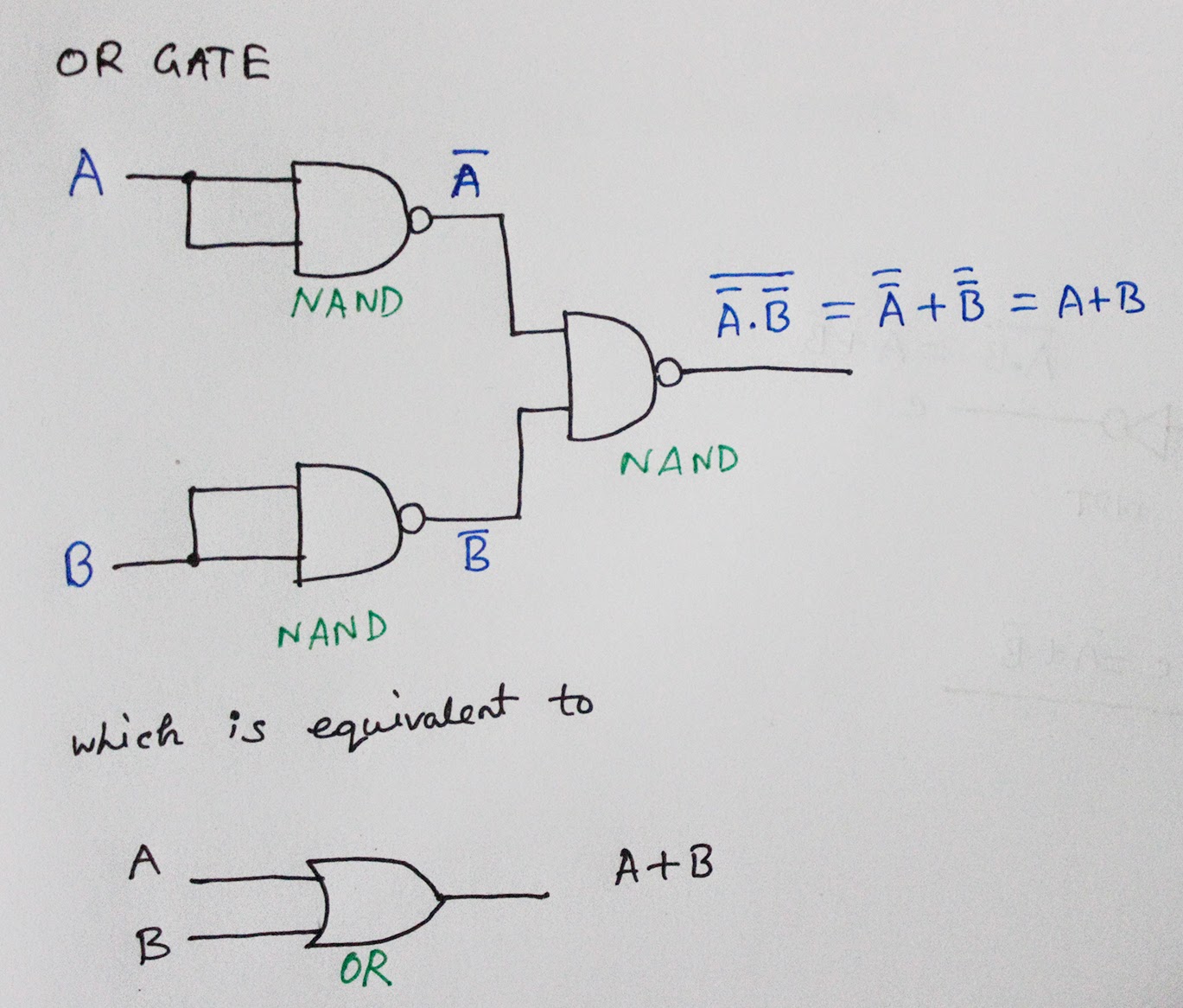
Conversion of NAND gate to Basic gates
Scavenger's Blog: NAND Gate

Nand Gate Schematic Diagram | wiring next project

(PDF) All Optical Logic NAND Gate Using Dark-Bright Soliton Conversion

☑ Diode Resistor Logic Nand Gate

Solved: Draw the schematic for a four-input NAND gate with a de

Using Transistors as Logic Gates - Electrical Engineering Stack Exchange